

Wie im einleitenden Artikel bereits beschrieben und angedeutet entstand so mit einem CPLD ein hochgenaues Kapazitätsmessgerät mit SPI Interface und einem Pyboard, welches dann alle Daten in ein Logfile schrieb.
Zur Anwendung kam hier ein MAX II EPM240T100 von Altera. Ein PyBoard welches über SPI die Daten empfing und diese in ein LogFile auf eine Speicherkarte schrieb.
Zuerst der Plan welcher mit Quartus erstellt wurde.
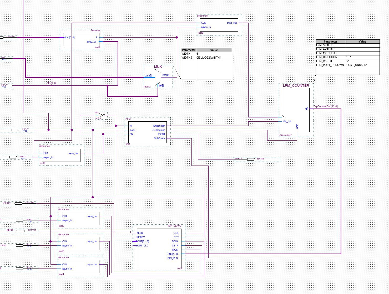
Links oben sind die 6 Kanäle, welche vom Pyboard ausgewählt werden können. Rechts oben die entsprechende Auswerteinheit und im unteren Teil die SPI Schnittstelle.Die FSM (Finite State Machine) ungefähr in der Mitte zur Steuerung der Funktionsblöcke.
Nur ein paar wenige bereits im Program enthaltene Funktionsblöcke (MUX, LPM_Counter) wurden verwendet.
Alles andere wurde in VHDL erstellt.
Der Decoder
library IEEE;
use IEEE.STD_LOGIC_1164.ALL;
use ieee.numeric_std.all;
entity Decoder is
port(E : in std_logic;
din : in std_logic_vector(2 downto 0);
dout : out std_logic_vector(5 downto 0));
end Decoder;
architecture descript of Decoder is
begin
process (E,din)
begin
if E='1' then
case din is
when "000" =>
dout <="000001";
when "001" =>
dout <="000010";
when "010" =>
dout <="000100";
when "011" =>
dout <="001000";
when "100" =>
dout <="010000";
when "101" =>
dout <="100000";
when others =>
dout <="000000";
end case;
else
dout <="000000";
end if;
end process;
end descript;
debounce ebenso
library IEEE;
use IEEE.STD_LOGIC_1164.ALL;
use IEEE.NUMERIC_STD.ALL;
entity debounce is
Port (
CLK : in std_logic; -- system clock
async_in : in std_logic; -- output data are valid
sync_out : out std_logic
);
end debounce;
architecture RTL of debounce is
signal ff1_out : std_logic;
--signal ff2_out : std_logic;
begin
process
begin -- Einsynchronisieren
wait until rising_edge(CLK);
ff1_out <= async_in;
sync_out <= ff1_out;
end process;
end RTL;
Die Finite State Machine zur Steuerung der Einzelnen Funktionsblöcke
library IEEE;
use IEEE.STD_LOGIC_1164.ALL;
use IEEE.NUMERIC_STD.ALL;
entity FSM is
Port (
rst : IN STD_LOGIC := '0';
clock : IN STD_LOGIC;
EN : IN STD_LOGIC := '0';
--counter : IN STD_LOGIC_VECTOR(23 DOWNTO 0) := "000000000000000000000000";
ENcounter : OUT STD_LOGIC;
CLRcounter : OUT STD_LOGIC;
EXTI4 : OUT STD_LOGIC;
--EN_input : OUT STD_LOGIC;
--EN_shift : OUT STD_LOGIC;
ShiftClock : OUT STD_LOGIC
--ShiftLoad : OUT STD_LOGIC
);
end FSM;
architecture Verhalten of FSM is
type state_t is (reset, idle, count_up, shift_load, shift_loadin, done); --EXTI_4,
signal state : state_t := idle;
signal counter : unsigned(25 downto 0) := "00000000000000000000000000";
begin
process begin
wait until rising_edge(clock);
ENcounter <= '0';
CLRcounter <= '0';
EXTI4 <= '0';
--EN_input <= '0';
--EN_shift <= '0';
ShiftClock <= '0';
--ShiftLoad <= '0';
case state is
when reset =>
counter <= (others=>'0');
state <= idle;
CLRcounter <= '1';
when idle =>
CLRcounter <= '1';
if (EN='1') then
state <= count_up;
else
state <= idle;
end if;
when count_up =>
CLRcounter <= '0';
ENcounter <= '1';
counter <= counter+1;
IF ((counter(25 DOWNTO 0) = "10111110101111000010000000")) THEN
---------5 000 00000000000001001110001000
--------50 000 00000000001100001101010000
-----50 000 00 00010011000100101101000000
----50 000 000 10111110101111000010000000
state <= shift_load;
-- Inserting 'else' block to prevent latch inference
ELSE
state <= count_up;
END IF;
when shift_load =>
ENcounter <= '0';
--EN_shift <= '1';
--ShiftLoad <= '1';
state <= shift_loadin;
when shift_loadin =>
--EN_shift <= '1';
--ShiftLoad <= '1';
ShiftClock <= '1';
--state <= EXTI_4;
state <= done;
--when EXTI_4 =>
--EN_shift <= '1';
--state <= done;
when done =>
EXTI4 <= '1';
state <= done;
end case;
if (rst='1') then
state <= reset;
end if;
end process;
--rowNr <= std_logic_vector(reg_rowNr);
--colNr <= std_logic_vector(reg_colNr);
--dout <= std_logic_vector(counter);
end Verhalten;
Nun fehlte mir noch das SPI Interface, welches aber nicht von mir geschrieben ist
von AUTHORS: Jakub Cabal :
--------------------------------------------------------------------------------
-- PROJECT: SPI MASTER AND SLAVE FOR FPGA
--------------------------------------------------------------------------------
-- NAME: SPI_SLAVE
-- AUTHORS: Jakub Cabal <jakubcabal@gmail.com>
-- LICENSE: LGPL-3.0, please read LICENSE file
-- WEBSITE: https://github.com/jakubcabal/spi-fpga
--------------------------------------------------------------------------------
-- COPYRIGHT NOTICE:
--------------------------------------------------------------------------------
-- SPI MASTER AND SLAVE FOR FPGA
-- Copyright (C) 2016 Jakub Cabal
--
-- This source file is free software: you can redistribute it and/or modify
-- it under the terms of the GNU Lesser General Public License as published by
-- the Free Software Foundation, either version 3 of the License, or
-- (at your option) any later version.
--
-- This source file is distributed in the hope that it will be useful,
-- but WITHOUT ANY WARRANTY; without even the implied warranty of
-- MERCHANTABILITY or FITNESS FOR A PARTICULAR PURPOSE. See the
-- GNU Lesser General Public License for more details.
--
-- You should have received a copy of the GNU Lesser General Public License
-- along with this program. If not, see <http://www.gnu.org/licenses/>.
--------------------------------------------------------------------------------library IEEE;
use IEEE.STD_LOGIC_1164.ALL;
use IEEE.NUMERIC_STD.ALL;-- THE SPI SLAVE MODULE SUPPORT ONLY SPI MODE 0 (CPOL=0, CPHA=0)!!!
entity SPI_SLAVE is
Port (
CLK : in std_logic; -- system clock
RST : in std_logic; -- high active synchronous reset
-- SPI SLAVE INTERFACE
SCLK : in std_logic; -- SPI clock
CS_N : in std_logic; -- SPI chip select, active in low
MOSI : in std_logic; -- SPI serial data from master to slave
MISO : out std_logic; -- SPI serial data from slave to master
-- USER INTERFACE
DIN : in std_logic_vector(31 downto 0); -- input data for SPI master
DIN_VLD : in std_logic; -- when DIN_VLD = 1, input data are valid
READY : out std_logic; -- when READY = 1, valid input data are accept
DOUT : out std_logic_vector(31 downto 0); -- output data from SPI master
DOUT_VLD : out std_logic -- when DOUT_VLD = 1, output data are valid
);
end SPI_SLAVE;architecture RTL of SPI_SLAVE is
signal spi_clk_reg : std_logic;
signal spi_clk_redge_en : std_logic;
signal spi_clk_fedge_en : std_logic;
signal bit_cnt : unsigned(4 downto 0);
signal bit_cnt_max : std_logic;
signal last_bit_en : std_logic;
signal load_data_en : std_logic;
signal data_shreg : std_logic_vector(31 downto 0);
signal slave_ready : std_logic;
signal shreg_busy : std_logic;
signal rx_data_vld : std_logic;begin
-- -------------------------------------------------------------------------
-- SPI CLOCK REGISTER
-- --------------------------------------------------------------------------- The SPI clock register is necessary for clock edge detection.
spi_clk_reg_p : process (CLK)
begin
if (rising_edge(CLK)) then
if (RST = '1') then
spi_clk_reg <= '0';
else
spi_clk_reg <= SCLK;
end if;
end if;
end process;-- -------------------------------------------------------------------------
-- SPI CLOCK EDGES FLAGS
-- --------------------------------------------------------------------------- Falling edge is detect when SCLK=0 and spi_clk_reg=1.
spi_clk_fedge_en <= not SCLK and spi_clk_reg;
-- Rising edge is detect when SCLK=1 and spi_clk_reg=0.
spi_clk_redge_en <= SCLK and not spi_clk_reg;-- -------------------------------------------------------------------------
-- RECEIVED BITS COUNTER
-- --------------------------------------------------------------------------- The counter counts received bits from the master. Counter is enabled when
-- falling edge of SPI clock is detected and not asserted CS_N.
bit_cnt_p : process (CLK)
begin
if (rising_edge(CLK)) then
if (RST = '1') then
bit_cnt <= (others => '0');
elsif (spi_clk_fedge_en = '1' and CS_N = '0') then
if (bit_cnt_max = '1') then
bit_cnt <= (others => '0');
else
bit_cnt <= bit_cnt + 1;
end if;
end if;
end if;
end process;-- The flag of maximal value of the bit counter.
bit_cnt_max <= '1' when (bit_cnt = "11111") else '0';-- -------------------------------------------------------------------------
-- LAST BIT FLAG REGISTER
-- --------------------------------------------------------------------------- The flag of last bit of received byte is only registered the flag of
-- maximal value of the bit counter.
last_bit_en_p : process (CLK)
begin
if (rising_edge(CLK)) then
if (RST = '1') then
last_bit_en <= '0';
else
last_bit_en <= bit_cnt_max;
end if;
end if;
end process;-- -------------------------------------------------------------------------
-- RECEIVED DATA VALID FLAG
-- --------------------------------------------------------------------------- Received data from master are valid when falling edge of SPI clock is
-- detected and the last bit of received byte is detected.
rx_data_vld <= spi_clk_fedge_en and last_bit_en;-- -------------------------------------------------------------------------
-- SHIFT REGISTER BUSY FLAG REGISTER
-- --------------------------------------------------------------------------- Data shift register is busy until it sends all input data to SPI master.
shreg_busy_p : process (CLK)
begin
if (rising_edge(CLK)) then
if (RST = '1') then
shreg_busy <= '0';
else
if (DIN_VLD = '1' and (CS_N = '1' or rx_data_vld = '1')) then
shreg_busy <= '1';
elsif (rx_data_vld = '1') then
shreg_busy <= '0';
else
shreg_busy <= shreg_busy;
end if;
end if;
end if;
end process;-- The SPI slave is ready for accept new input data when CS_N is assert and
-- shift register not busy or when received data are valid.
slave_ready <= (CS_N and not shreg_busy) or rx_data_vld;
-- The new input data is loaded into the shift register when the SPI slave
-- is ready and input data are valid.
load_data_en <= slave_ready and DIN_VLD;-- -------------------------------------------------------------------------
-- DATA SHIFT REGISTER
-- --------------------------------------------------------------------------- The shift register holds data for sending to master, capture and store
-- incoming data from master.
data_shreg_p : process (CLK)
begin
if (rising_edge(CLK)) then
if (load_data_en = '1') then
data_shreg <= DIN;
elsif (spi_clk_redge_en = '1' and CS_N = '0') then
data_shreg <= data_shreg(30 downto 0) & MOSI;
end if;
end if;
end process;-- -------------------------------------------------------------------------
-- MISO REGISTER
-- --------------------------------------------------------------------------- The output MISO register ensures that the bits are transmit to the master
-- when is not assert CS_N and falling edge of SPI clock is detected.
miso_p : process (CLK)
begin
if (rising_edge(CLK)) then
if (load_data_en = '1') then
MISO <= DIN(31);
elsif (spi_clk_fedge_en = '1' and CS_N = '0') then
MISO <= data_shreg(31);
end if;
end if;
end process;-- -------------------------------------------------------------------------
-- ASSIGNING OUTPUT SIGNALS
-- -------------------------------------------------------------------------
READY <= slave_ready;
DOUT <= data_shreg;
DOUT_VLD <= rx_data_vld;end RTL;
So nun fehlt nur noch das PyBoard
# main.py -- put your code here!
import pyb
from pyb import Pin
import math, micropython, array
import stm
from stm import mem32
debug=0
#PA0 > 8 MOSI EN - in
#PC0 > 7 EN - in
#PC1 < 4 EXTI4 - out
#PA1 > 1 MSCK -in
#PC2 < 3 MISO
#PA2 > 27 sel2
#PA3 > 28 sel1
#PA4 > 29 sel0
MISO_EN=Pin('A0',Pin.OUT)
EN=Pin('C0',Pin.OUT)
MSCK=Pin('A1',Pin.OUT)
MISO = Pin('C2', Pin.IN)
EXTI4 = Pin('C1', Pin.IN)
sel3=Pin('A5',Pin.OUT)
#!!!!!!!!!!!!!!!!!!!!!!!!!!!!!!!!!!!!!!!!!! change top down TODO
sel2=Pin('A2',Pin.OUT)
sel1=Pin('A3',Pin.OUT)
sel0=Pin('A4',Pin.OUT)
chn=0
sel2.value(0)
sel1.value(0)
sel0.value(0)
channel_firstrun=[0,0,0,0,0,0]
channel_mask=[1,1,0,0,1,1]
channel_erg=[0,0,0,0,0,0,0,0,0,0,0,0]
channel_mittel=[0,0,0,0,0,0]
MISO_EN.value(1)
#MISO_EN.value(0)
EN.value(1)
varEXTI4=EXTI4.value()
MSCK.value(0)
MISO.value()
#x=[0,0,0,0,0,0,0,0,0,0,0,0,0,0,0,0,0,0,0,0,0,0,0,0,0,0,0,0,0,0,0,0]
pyb.LED(1).on()
pyb.delay(4000)
pyb.LED(1).off()
pyb.LED(2).off()
pyb.LED(3).off()
pyb.LED(4).off()
#print(x)
blue = pyb.LED(4)
switch = pyb.Switch()
irq_request=0
firstrun=0
mittel=0
log = open('/sd/log.csv', 'w')
# loop
while not switch(): #True:
# wait for interrupt
# this reduces power consumption while waiting for switch press
#pyb.wfi()
# start if switch is pressed
#if switch():
pyb.LED(1).on() # blue LED indicates file open
# delay avoids detection of multiple presses
if chn > 5:
chn=0
if debug>0:
print(channel_erg)
log.write('{}\n'.format(channel_erg)) # write data to file
channel_erg=[0,0,0,0,0,0,0,0,0,0,0,0]
if debug==1:
print(chn)
if chn==0:
sel2.value(0)
sel1.value(0)
sel0.value(0)
if chn==1:
sel2.value(0)
sel1.value(0)
sel0.value(1)
if chn==2:
sel2.value(0)
sel1.value(1)
sel0.value(0)
if chn==3:
sel2.value(0)
sel1.value(1)
sel0.value(1)
if chn==4:
sel2.value(1)
sel1.value(0)
sel0.value(0)
if chn==5:
sel2.value(1)
sel1.value(0)
sel0.value(1)
EN.value(0)
pyb.delay(10)
pyb.LED(3).off()
pyb.delay(200)
pyb.LED(3).on()
EN.value(1)
#~ while not EXTI4.value(): #warte auf interupt
#~ pyb.LED(3).off()
#~ pyb.delay(200)
#~ pyb.LED(3).on()
#~ pyb.delay(200)
pyb.delay(2000)
pyb.LED(3).off()
n=0
z=1
MISO_EN.value(0)
MSCK.value(0)
xf=[0,0,0,0,0,0,0,0,0,0,0,0,0,0,0,0,0,0,0,0,0,0,0,0,0,0,0,0,0,0,0,0]
#x=[0,0,0,0,0,0,0,0,0,0,0,0,0,0,0,0,0,0,0,0,0,0,0,0,0,0,0,0,0,0,0,0]
for i in range(31):
pyb.delay(1)
MSCK.value(1)
pyb.delay(1)
MSCK.value(0)
pyb.delay(1)
xf[i+1]=MISO.value()
z=1
MISO_EN.value(1)
for i in range(31):
hn=xf[31-i]
if hn== 1:
n=n+z
z=z*2
if n>4000000:
channel_mask[chn] =0
if debug==1:
print(channel_mask)
#if 200<n<600000:
if channel_firstrun[chn]==0:
#if firstrun==0:
#mittel=32*n
channel_mittel[chn]=n
firstrun=1
channel_firstrun[chn]=1
print("first run")
print(channel_firstrun)
mittel=channel_mittel[chn]
mittel_tmp=mittel*32
#if mittel_tmp-10000<n<mittel_tmp+10000:
#mittel=mittel_tmp-mittel+n
#erg=mittel/32
erg=(mittel_tmp-mittel+n)/32
channel_mittel[chn]=erg
channel_erg[chn*2]=n
channel_erg[chn*2+1]=erg
#print(n,erg,chn)
#log.write('{},{},{}\n'.format(n,erg,chn)) # write data to file
# chn erhöhen
chn=chn+1
if chn<5:
while channel_mask[chn] == 0:
chn=chn+1
#end if
#print(chn,channel_mask,channel_erg)
pyb.LED(1).off() # blue LED indicates file closed
pyb.delay(200) # delay avoids detection of multiple presses
log.close() # close file
pyb.LED(1).on()
pyb.LED(2).on()
pyb.LED(3).on()
pyb.LED(4).on()
pyb.delay(10000)
pyb.LED(1).off()
pyb.LED(2).off()
pyb.LED(3).off()
pyb.LED(4).off()
Entsprechend dem Plan wurden beide DevBoards miteinander verkabelt.
#PA0 > 8 MOSI EN - in
#PC0 > 7 EN - in
#PC1 < 4 EXTI4 - out
#PA1 > 1 MSCK -in
#PC2 < 3 MISO
#PA2 > 27 sel2
#PA3 > 28 sel1
#PA4 > 29 sel0
und los ging es mit Messungen
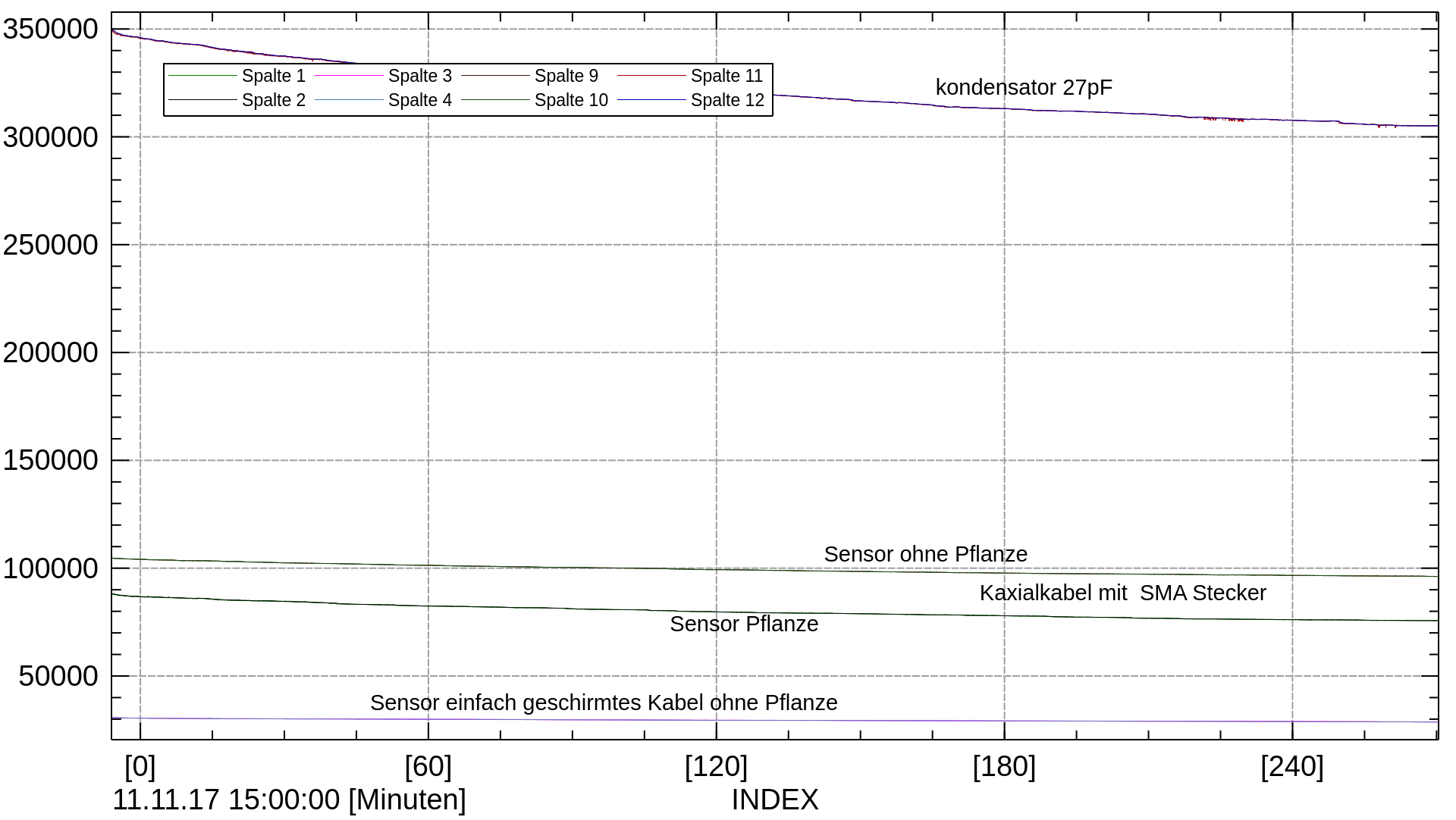
Sehr schön im unteren Teil zu erkennen ist dass es SO GUT WIE KEIN UNTERSCHIED an den Sensoren im Verlauf gibt. Ob mit oder ohne Pflanze.
Nur die Temperaturabhängigkeit ist am Keramikkondensator am stärksten.
Aber nochmal zurück zur reinen PflanzenSensor Messung
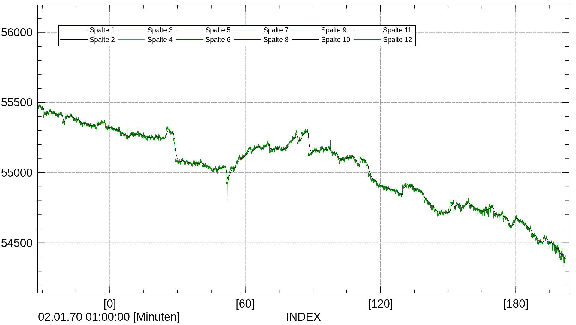
Hier besonders schön zu sehen sind die Schwankungen,
Ergebnis dieses Projektes
Eine kapazitive Messung der Bodenfeuchte ist nur in einer speziell geeichten Erde kurzzeitig möglich.
Über einen längeren Messzeitraum verändern sich die Werte bereits mit dem Wasser selbst. Kalk und Salzgehalt spielen dabei eine entscheidende Rolle und wenn dann noch Flüssigdünger mit ins Spiel kommt, kann eine Vorhersage, wann gegossen werden soll nicht mehr bestimmt werden.


- Anmelden, um Kommentare verfassen zu können